- 您现在的位置:买卖IC网 > Sheet目录989 > MAX1234EVC16 (Maxim Integrated Products)EV SYSTEM/EV KIT MAX1233/MAX1234
�� �
�
�±15kV� ESD-Protected� Touch-Screen�
�Controllers� Include� DAC� and� Keypad� Controller�
�ment,� temperature� measurement,� or� auxiliary� input�
�measurement� is� written� to� the� ADC� control� register,� the�
�device� powers� on� the� internal� reference,� waits� for� the�
�+1.25V�
�BANDGAP�
�internal� reference� to� settle,� completes� the� requested�
�scan,� and� powers� down� the� internal� reference.� The� ref-�
�3R�
�2x�
�REF� PIN�
�OPTIONAL�
�erence� power� delay� depends� upon� the� ADC� resolution�
�selected� (see� Table� 8).� Do� not� bypass� REF� with� an�
�external� capacitor� when� performing� scans� in� auto�
�power-down� mode.�
�2R�
�Full-Power� Mode� (RES1� =� 0,� RES0� =� 1)�
�In� the� full-power� mode,� the� RES1� bit� is� set� LOW� and�
�RES0� bit� is� set� HIGH.� In� this� mode,� the� device� is� pow-�
�ered� up� and� the� internal� ADC� reference� is� always� ON.�
�The� MAX1233/MAX1234� internal� reference� remains� fully�
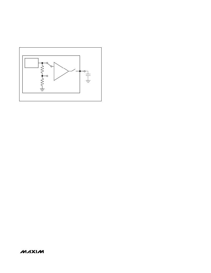
�Figure� 4.� Block� Diagram� of� the� Internal� Reference�
�measurement� of� the� auxiliary� inputs.� Figure� 4� shows� the�
�on-chip� reference� circuitry� of� the� MAX1233/MAX1234.�
�Set� the� internal� reference� voltage� by� writing� to� the� RFV�
�bits� in� the� ADC� control� register� (see� Tables� 4,� 5,� and� 12).�
�The� MAX1233/MAX1234� can� accept� an� external� refer-�
�ence� connected� to� REF� for� ADC� conversion.�
�External� Reference�
�The� MAX1233/MAX1234� can� accept� an� external� refer-�
�ence� connected� to� the� REF� pin� for� ADC� conversions.�
�The� internal� reference� should� be� disabled� (RES1� =� 1)�
�when� using� an� external� reference.� At� a� conversion� rate�
�of� 50ksps,� an� external� reference� at� REF� must� deliver� up�
�to� 15μA� of� load� current� and� have� 50� Ω� or� less� output�
�impedance.� If� the� external� reference� has� high� output�
�impedance� or� is� noisy,� bypass� it� close� to� the� REF� pin�
�with� a� 0.1μF� capacitor.�
�Selecting� Internal� or� External� Reference�
�Set� the� type� of� reference� being� used� by� programming�
�the� ADC� control� register.� To� select� the� internal� refer-�
�ence,� clock� zeros� into� bits� [A/D3:A/D0]� and� a� zero� to� bit�
�RES1,� as� shown� in� the� Control� Registers� section.� To�
�change� to� external� reference� mode,� clock� zeros� into�
�bits� [A/D3:A/D0]� and� a� one� to� bit� RES1.� See� Table� 13�
�for� more� information� about� selecting� an� internal� or�
�external� reference� for� the� ADC.�
�Reference� Power� Modes�
�Auto� Power-Down� Mode� (RES1� =� RES0� =� 0)�
�The� MAX1233/MAX1234� are� in� auto� power-down� mode�
�at� initial� power-up.� Set� the� RES1� and� RES0� bits� to� zero�
�to� use� the� MAX1233/MAX1234� in� the� auto� power-down�
�mode.� In� this� mode,� the� internal� reference� is� normally�
�off.� When� a� command� to� perform� a� battery� measure-�
�powered� after� completing� a� scan.�
�Internal� Clock�
�The� MAX1233/MAX1234� operate� from� an� internal� oscil-�
�lator,� which� is� accurate� to� within� 20%� of� the� 10MHz�
�specified� clock� rate.� The� internal� oscillator� controls� the�
�timing� of� the� acquisition,� conversion,� touch-screen� set-�
�tling,� reference� power-up,� and� keypad� debounce� times.�
�8-Bit� DAC�
�The� MAX1233/MAX1234� have� a� voltage-output,� true� 8-bit�
�monotonic� DAC� with� less� than� 1LSB� integral� nonlinearity�
�error� and� less� than� 1LSB� differential� nonlinearity� error.� It�
�requires� a� supply� current� of� only� 150μA� (typ)� and� pro-�
�vides� a� buffered� voltage� output.� The� DAC� is� at� midscale�
�code� at� power-up� and� remains� there� until� a� new� code� is�
�written� to� the� DAC� register.� During� shutdown,� the� DAC’s�
�output� is� pulled� to� ground� with� a� 1M� Ω� load.�
�The� internal� DAC� can� be� used� in� various� system� applica-�
�tions� such� as� LCD/TFT-bias� control,� automatic� tuning�
�(VCO),� power� amplifier� bias� control,� programmable�
�threshold� levels,� and� automatic� gain� control� (AGC).�
�The� 8-bit� DAC� in� the� MAX1233/MAX1234� employs� a�
�current-steering� topology� as� shown� in� Figure� 5.� At� the�
�core� of� this� DAC� is� a� reference� voltage-to-current� con-�
�verter� (V/I)� that� generates� a� reference� current.� This� cur-�
�rent� is� mirrored� to� 255� equally� weighted� current�
�sources.� DAC� switches� control� the� outputs� of� these� cur-�
�rent� mirrors� so� that� only� the� desired� fraction� of� the� total�
�current-mirror� currents� is� steered� to� the� DAC� output.�
�The� current� is� then� converted� to� a� voltage� across� a�
�resistor,� and� the� output� amplifier� buffers� this� voltage.�
�DAC� Output� Voltage�
�The� 8-bit� DAC� code� is� binary� unipolar� with� 1LSB� =�
�(V� REF� /256).� The� DAC� has� a� full-scale� output� voltage� of�
�(0.9� � AV� DD� -� 1LSB).�
�______________________________________________________________________________________�
�15�
�发布紧急采购,3分钟左右您将得到回复。
相关PDF资料
MAX1402EVC16
EVAL KIT FOR MAX1402
MAX16802BEVKIT
EVAL KIT FOR MAX16802
MAX16803EVKIT+
EVAL KIT FOR MAX16803
MAX16806EVMAXQUSB+
EVAL KIT FOR MAX16806
MAX16807EVKIT+
EVAL KIT FOR MAX16807
MAX16809EVKIT+
EVAL KIT FOR MAX16809
MAX16814EVKIT+
KIT EAL FOR MAX16814
MAX16816EVKIT+
KIT EVAL FOR MAX16816 LED DRIVER
相关代理商/技术参数
MAX1234EVKIT
制造商:Maxim Integrated Products 功能描述:+15KV ESD-PROTECTED TOUCH-SCREEN CO - Rail/Tube
MAX1236EUA
功能描述:模数转换器 - ADC RoHS:否 制造商:Texas Instruments 通道数量:2 结构:Sigma-Delta 转换速率:125 SPs to 8 KSPs 分辨率:24 bit 输入类型:Differential 信噪比:107 dB 接口类型:SPI 工作电源电压:1.7 V to 3.6 V, 2.7 V to 5.25 V 最大工作温度:+ 85 C 安装风格:SMD/SMT 封装 / 箱体:VQFN-32
MAX1236EUA+
功能描述:模数转换器 - ADC 12-Bit 4Ch 94.4ksps 5.5V Precision ADC RoHS:否 制造商:Texas Instruments 通道数量:2 结构:Sigma-Delta 转换速率:125 SPs to 8 KSPs 分辨率:24 bit 输入类型:Differential 信噪比:107 dB 接口类型:SPI 工作电源电压:1.7 V to 3.6 V, 2.7 V to 5.25 V 最大工作温度:+ 85 C 安装风格:SMD/SMT 封装 / 箱体:VQFN-32
MAX1236EUA+T
功能描述:模数转换器 - ADC 12-Bit 4Ch 94.4ksps 5.5V Precision ADC RoHS:否 制造商:Texas Instruments 通道数量:2 结构:Sigma-Delta 转换速率:125 SPs to 8 KSPs 分辨率:24 bit 输入类型:Differential 信噪比:107 dB 接口类型:SPI 工作电源电压:1.7 V to 3.6 V, 2.7 V to 5.25 V 最大工作温度:+ 85 C 安装风格:SMD/SMT 封装 / 箱体:VQFN-32
MAX1236EUA-T
功能描述:模数转换器 - ADC RoHS:否 制造商:Texas Instruments 通道数量:2 结构:Sigma-Delta 转换速率:125 SPs to 8 KSPs 分辨率:24 bit 输入类型:Differential 信噪比:107 dB 接口类型:SPI 工作电源电压:1.7 V to 3.6 V, 2.7 V to 5.25 V 最大工作温度:+ 85 C 安装风格:SMD/SMT 封装 / 箱体:VQFN-32
MAX1236EVKIT
功能描述:数据转换 IC 开发工具 MAX1236 Eval Kit RoHS:否 制造商:Texas Instruments 产品:Demonstration Kits 类型:ADC 工具用于评估:ADS130E08 接口类型:SPI 工作电源电压:- 6 V to + 6 V
MAX1236KEUA
功能描述:模数转换器 - ADC RoHS:否 制造商:Texas Instruments 通道数量:2 结构:Sigma-Delta 转换速率:125 SPs to 8 KSPs 分辨率:24 bit 输入类型:Differential 信噪比:107 dB 接口类型:SPI 工作电源电压:1.7 V to 3.6 V, 2.7 V to 5.25 V 最大工作温度:+ 85 C 安装风格:SMD/SMT 封装 / 箱体:VQFN-32
MAX1236KEUA+
功能描述:模数转换器 - ADC RoHS:否 制造商:Texas Instruments 通道数量:2 结构:Sigma-Delta 转换速率:125 SPs to 8 KSPs 分辨率:24 bit 输入类型:Differential 信噪比:107 dB 接口类型:SPI 工作电源电压:1.7 V to 3.6 V, 2.7 V to 5.25 V 最大工作温度:+ 85 C 安装风格:SMD/SMT 封装 / 箱体:VQFN-32